
Structural Properties Of Si:H Thin Fılm Grown By VHF- PEDVD

Abstract
Hydrogenated silicon (Si:H) thin film is one of the most promising technology that has been developed throughout the years. The film structure possess a variety of traits, especially in semiconductor and solar cell industry; depends on its molecule condition either in crystal or amorphous state. Plasma Enhanced Chemical Vapour Deposition (PECVD) technique is chosen in this work as it may give high quality of silicon thin film at lower temperature compared to conventional Chemical Vapour Deposition (CVD) technique. This work aims to study the transition of silicon thin film from amorphous to crystal as the effect of very high RF frequency (VHF) deposition. Three frequencies were used throughout the experiment; 100 MHz, 160MHZ and 200 MHz. The films were deposited for 15 minutes on Boron doped Si (100) substrate while the temperature, power density and gaseous flowrate were kept constant. Raman spectroscopy, Fourier Transform Infrared (FTIR) and Atomic Force Microscopy (AFM) were used as characterization techniques. The results shown that significant dependence of Si:H film with VHF as the transition occurs from amorphous to crystalline along with rough surface as deposition frequency increases while from FTIR results, the amount of Si:H shown an increment with the increased in frequency.
Keywords: VHF-PECVDHydrogenated Silicon Thin FilmRaman SpectroscopyFTIR
Introduction
Hydrogenated Silicon (Si:H) thin film is a well-known technology that has been developed throughout the years. High performance of Si:H has benefits many industries especially for solar cell industries, semiconductor industries and even for Micro-Electro Mechanical System (MEMS) (Martinu, Zabeida, & Klemberg-Sapieha, 2010; Iliescu et al., 2011; Kondo & Matsuda, 2001; Lien et al., 2010). The nano-structure and morphology study becoming the centre of attention in this study since these information may give better understanding in film fabrication and its affect from Very High Frequency (VHF) deposition.
Plasma Enhanced Chemical Vapour Deposition (PECVD) is chosen due to its capability to grow Si:H film at much lower temperature, compared to conventional CVD (Kondo & Matsuda, 2001). As plasma discharge from coupled capacitor in the chamber, the gas reactants will be dissociated and formed and undergo several chemical reactions before finally deposit onto the substrate. At higher RF frequency, the deposition rate is higher and better deposition could be achieved due to high amount of electron density compared to conventional plasma excitation frequency, 13.56 MHz (Matsuda, 2004; Heintze, Zedlitz, & Bauer, 1993; Das, Jana, & Ray, 2004). As a result, by varying the excitation frequency, different type of Si:H will be deposited. According to Fukawa, Suzuki, Guo, and Kondo, the transition from amorphous hydrogenated silicon (a-Si:H) to crystalline hydrogenated silicon (c-Si:H) will occur as the deposition frequency increased (2001). As time pass by, the continuation of much higher frequency is needed in order to give better information in term of crystallinity, chemical bonding of Si:H and its morphology for further references.
Problem Statement
Si thin film can be existing in both crystalline and amorphous state, depending on the parameters set for the deposition. There are many possible parameters that can be altered to obtain Si crystal deposition. Even in low deposition frequency, crystalline Si still can be produced by having higher substrate temperature, which is around 200 oC and above; high hydrogen dilution ratio and high deposition pressure (Kondo & Matsuda, 2001; Guo, Ding, Yang, Ling, & Cheng, 2011 ; Johnson, Kroely, & Roca I Cabarrocas, 2009; Kondo et al., 2000). However, the crystallinity still become unknown if the deposition frequency that will be used is around 200 MHz. The surface roughness also can be related with the crystallinity of the sample, as it can affect the solar cell performance (Brinza, Rath, & Schropp, 2009; Isabella, Krč, & Zeman, 2010; Scholtz, Ladanyi, & Mullerova, 2014). The amount of Hydrogen content in Si:H also remain unclear in the VHF deposition..
Research Questions
The PECVD deposition technique is a well-known technique to grow a thin film, especially at conventional frequency (13.56 MHz). However at the range of VHF, there are still little studies that have been done especially at 200 MHz. Therefore, this experiment is done based on the main question regarding on what type of Si:H film will be grown at this particular frequency. This included the morphology study, the amount of hydrogen in the film and the crystallinity of the film.
Purpose of the Study
The main objective for this study is to relate the VHF-PECVD deposition of silicon thin film and the crystallinity of the Si:H film. The next objective is to find the surface roughness for each film by having morphology study and the last objective is to have the amount of hydrogen in the Si:H film for each deposition frequency.
Research Methods
Boron doped silicon substrate with (100) orientation was used as substrate, with 1 cm x 1 cm dimension. First, the substrates were cleaned with standard cleaning process. Three deposition frequencies were chosen which were 100 MHz, 160 MHz and 200 MHz with Argon (Ar) as source of plasma. The silicon film then was deposited for 15 minutes, with constant stage temperature, 180 oC. Hydrogen dilution ratio (H2/SiH4) was maintained with 10 throughout the experiment for sample 160 MHz and 200 MHz, with 100 sscm and 10 sscm; while for 100 MHz sample, 80 sscm and 8 sscm was chosen. The deposition pressure ranged between 2.x10-2 torr to 6.10-1 torr.
Characterizations and analysis were performed to give better understanding on the effect of frequencies to Si:H film. First, Raman spectroscopy analysis was carried out to represent the transition of Si:H film from a-Si:H to c-Si:H. The sample was excited by using 532 nm laser in order to get Raman spectra shift. The morphology study was performed by Atomic Force Microscopy (AFM) with 1 μm resolution. This analysis provides data regarding surface roughness alongside with the grain size for each sample. Finally, the chemical bonding analysis was carried out using Attenuated Total Reflectance Fourier-Transform Infrared spectroscopy (ATR-FTIR) which focus only for Si:H bond
Findings
In this section, all data will be discussed and reviewed to match the objectives of this experiment.
Raman Spectra Analysis
In Raman spectra analysis, the significant peaks for Si:H film are located around 480 cm-1, 500 cm-1 and 520 cm-1. Generally, broad Gaussian peak at 480 cm-1 represents to a-Si:H, while 500 cm-1 refers to the combination of a-Si:H and c-Si:H and the sharp peak at 520 cm-1 as c-Si:H (Mukhopadhyay, Das, & Ray, 2004; Lyon & Nemanich, 1983). Figure
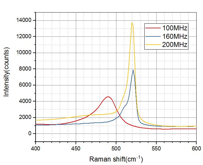
For Si:H film grown by 100 MHz, the results clearly shown that only a-Si:H existed on the substrate. As the deposition frequency increased to 160 MHz and 200 MHz, the 480 cm-1 peak disappeared and significant peaks were found at 500 cm-1 and 520 cm-1. This clearly states that film grown at 160 MHz and 200 MHz are in crystal state compared to 480 cm-1. Raman crystallinity,
Xc = ([I520) / (I520+I500+I480) (1)
whereby,
AFM Analysis
The morphology study has been carried out for all the samples in order to provide better information regarding surface roughness and grain size. Figure
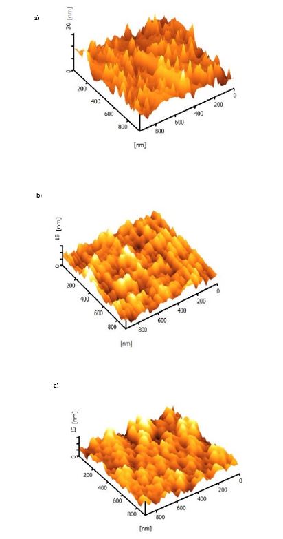
Ideally, crystalline film has rougher surface compare to amorphous as the grain size increased. Therefore, the morphology study from Table
ATR-FTIR Analysis
Deposition of Si:H on the substrate may varied from one to another sample. This is due to the dissociation of precursor gas SiH4 and H2 in the chamber at different frequency of plasma and different amount of hydrogen flowrate for 100 MHz sample, compared to 160 MHz and 200 MHz. Figure
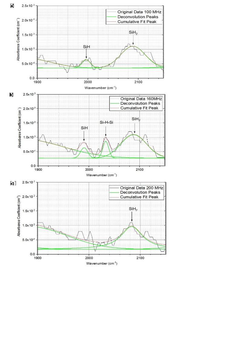
The Peaks ranging from 1950 cm-1 to 2100 cm-1 were analysed to study the bonding of Si:H. This range of frequency is chosen due to its capability to determine the amount of Hydrogen content (Langford, Fleet, Nelson, Lanford, & Maley, 1992). The results agreed with Raman results, as the crystallinity increased, the amount of monohydride Si:H decreased (Langford et al., 1992; Samanta & Das, 2017). By referring to Figure
NH = A2100SiHI2100SiH + A2000I2000 (2)
whereby
and
; the proportional factor for IR stretching modes while
and
are the intensity at the respective spectra (Langford et al., 1992). Table
As stated in Table
Conclusion
Three sets of samples consist of a-Si:H and c-Si:H have been successfully deposited using VHF-PECVD. The VHF plasma excitation frequency significantly affects the crystallinity of the Si:H film. As the frequency increases, tendency to form c-Si:H is much greater compared to a-Si:H. This has been proven by analysis in Raman spectroscopy by shifting peak from
Acknowledgments
It is an honour to have this particular study to present current progress of Silicon thin film study. We would express our gratitude especially to Ministry of Education for funding us with Fundamental Research Grant Scheme (FRGS) with grant entitled Investigation on Growth Kinetics and Properties of One-Dimensional Silicon Carbide Nanostructures Synthesis by Ultra High Frequency (UHF)-PECVD (R.J130000.7826.4F847) and also to Universiti Teknologi Malaysia by Research University Grant (GUP) entitled Structural And Optical Properties Of SiC Nanowires grown by VHF-PECVD (Q.J130000.2526.15H46). We also sincerely thank to Ibnu Sina Institute for Scientific and Industrial Research (ISIR), Universiti Teknologi Malaysia and all the staff for giving us valuable support and help during this study. We hope by having these knowledge, researcher may gain benefits in order to improve current technology by implementing VHF in film deposition technique.
References
- Altmannshofer, S., Miller, B., Holleitner, A. W., Boudaden, J., Eisele, I., & Kutter, C. (2018). Deposition of micro crystalline silicon films using microwave plasma enhanced chemical vapor deposition. Thin Solid Films, 645(September 2017), 180–186.
- Brinza, M., Rath, J. K., & Schropp, R. E. I. (2009). Thin film silicon n-i-p solar cells deposited by VHF PECVD at 100 oC substrate temperature. Solar Energy Materials and Solar Cells, 93(6–7), 680–683.
- Das, C., Jana, T., & Ray, S. (2004). Optoelectronic and Structural Properties of Undoped Microcrystalline Silicon Thin Films: Dependence on Substrate Temperature in Very High Frequency Plasma Enhanced Chemical Vapor Deposition Technique. Japanese Journal of Applied Physics, 43, 3269–3274.
- Fukawa, M., Suzuki, S., Guo, L., & Kondo, M. (2001). High rate growth of microcrystalline silicon using a high-pressure depletion method with VHF plasma, 66, 217–223.
- Guo, L., Ding, J., Yang, J., Ling, Z., & Cheng, G. (2011). Nanostructure , electrical and optical properties of p-type hydrogenated nanocrystalline silicon fi lms q. Vaccum, 85(6), 649–653.
- Heintze, M., Zedlitz, R., & Bauer, G. H. (1993). Analysis of high-rate a-si:H deposition in a vhf plasma. Journal of Physics D: Applied Physics, 26(10), 1781–1786.
- Iliescu, C., Avram, M., Chen, B., Popescu, A., Dumitrescu, V., Poenar, D. P., … Sterian, P. (2011). Residual stress in thin films PECVD depositions: A review. Journal of Optoelectronics and Advanced Materials, 13(4), 387–394.
- Isabella, O., Krč, J., & Zeman, M. (2010). Modulated surface textures for enhanced light trapping in thin-film silicon solar cells. Applied Physics Letters, 97(10).
- Jadhavar, A., Pawbake, A., Waykar, R., Jadkar, V., Kulkarni, R., Bhorde, A., … Jadkar, S. (2017). Growth of Hydrogenated Nano-crystalline Silicon (nc-Si:H) Films by Plasma Enhanced Chemical Vapor Deposition (PE-CVD). Energy Procedia, 110(December 2016), 45–52.
- Johnson, E. V., Kroely, L., & Roca i Cabarrocas, P. (2009). Raman scattering analysis of SiH bond stretching modes in hydrogenated microcrystalline silicon for use in thin-film photovoltaics. Solar Energy Materials and Solar Cells, 93(10), 1904–1906.
- Kondo, M., Fukawa, M., Guo, L., & Matsuda, A. (2000). High rate growth of microcrystalline silicon at low temperatures, 269, 84–89.
- Kondo, M., & Matsuda, A. (2001). Low temperature growth of microcrystalline silicon and its application to solar cells, 4–9.
- Langford, A. A., Fleet, M. L., Nelson, B. P., Lanford, W. A., & Maley, N. (1992). Infrared absorption strength and hydrogen content of hydrogenated amorphous silicon. Physical Review B, 45(23), 13367–13377.
- Lien, S. Y., Ou, Y. C., Cho, Y. S., Wang, C. C., Chen, C. F., Sun, W. C., & Wuu, D. S. (2010). Fabrication and chrarcterization silicon thin film solar cells deposited by HF-PECVD. Conference Record of the IEEE Photovoltaic Specialists Conference, 1545–1548.
- Lyon, S. A., & Nemanich, R. J. (1983). Raman scattering from hydrogenated amorphous silicon. Physica B+C, 117–118, 871–873.
- Martinu, L., Zabeida, O., & Klemberg-Sapieha, J. E. (2010). Plasma-Enhanced Chemical Vapor Deposition of Functional Coatings. Handbook of Deposition Technologies for Films and Coatings, 532–553.
- Matsuda, A. (2004). Thin-Film Silicon –Growth Process and Solar Cell Application–. Japanese Journal of Applied Physics, 43(12), 7909–7920.
- Mossad, A., & Kobayashi, H. (2014). Hydrogen effect on nanostructural features of nanocrystalline silicon thin fi lms deposited at 200 ° C by PECVD. Journal of Non-Crystalline Solids, 385, 17–23.
- Mukhopadhyay, S., Das, C., & Ray, S. (2004). Structural analysis of undoped microcrystalline silicon thin films deposited by PECVD technique. Journal of Physics D-Applied Physics, 37(13), 1736–1741. http://doi.org/Pii s0022-3727(04)71498-9\r
- Samanta, S., & Das, D. (2017). Nanocrystalline silicon thin fi lms from SiH 4 plasma diluted by H 2 and He in. Journal of Physical and Chemistry of Solids, 105(November 2016), 90–98.
- Scholtz, L., Ladanyi, L., & Mullerova, J. (2014). Influence of Surface Roughness on Optical Characteristics of Multilayer Solar Cells, 631–638.
Copyright information

This work is licensed under a Creative Commons Attribution-NonCommercial-NoDerivatives 4.0 International License.
About this article
Publication Date
17 May 2019
Article Doi
eBook ISBN
978-1-80296-061-7
Publisher
Future Academy
Volume
62
Print ISBN (optional)
-
Edition Number
1st Edition
Pages
1-539
Subjects
Business, innovation, sustainability, environment, green business, environmental issues
Cite this article as:
Omar, M. F., Ismail, A. K., & Rosman*, N. H. K. (2019). Structural Properties Of Si:H Thin Fılm Grown By VHF- PEDVD. In M. Imran Qureshi (Ed.), Technology & Society: A Multidisciplinary Pathway for Sustainable Development, vol 62. European Proceedings of Social and Behavioural Sciences (pp. 515-523). Future Academy. https://doi.org/10.15405/epsbs.2019.05.02.51